Solution
Zhengye New Products - Picosecond Laser Cutting Machine (Semiconductor)
Semiconductor industry gospel! The company has developed a high-precision and high-efficiency picosecond laser cutting technology that can be used in large-scale semiconductor wafer packaging and testing field, promoted the industry's technology upgrades, reduced cost.
R & D background
Driven by consumer applications such as smart phones, smart cards and stacked packaging, the demand for thin wafers is growing in recent years. And with the electronic products more and more towards the direction of precision, the market demand for high-precision processing is increasing, to promote a more accurate laser precision machining technology development.
To meet the needs of the market, is the technology research and development of picosecond laser cutting machine, deep plowing electronic information industry in the field of intelligent manufacturing.

Application areas
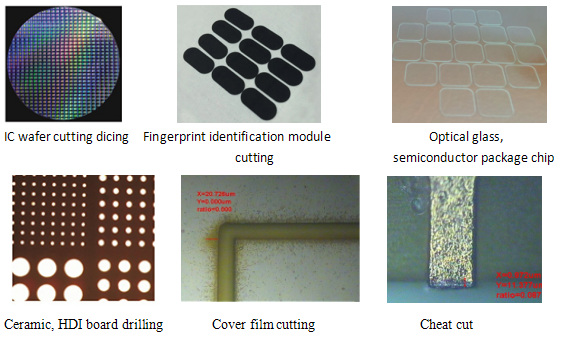
The equipment used in PCB / FPC industry cutting, drilling, to meet the cover film, cheat, soft board shape and other materials, precision cutting needs, but also can be used in glass, ceramics, wafers and other high-precision high-quality cutting needs.
Suitable for a variety of demanding fine precision, sensitive non-destructive, clean and smooth cutting requirements, to "cold processing" features, to solve the ceramic, silicon, glass, sapphire, thin, brittle, hard materials, metal, polymer and other sensitive materials and a variety of sticky, leather, tough materials processing problems.
Technical advantages
With the market's existing nanosecond laser technology, picosecond laser technology with a variety of advanced technology advantages, is the market trend.
1. processing speed is faster
Picosecond laser technology using 400kHz picosecond laser (1 ~ 1000kHz adjustable), galvanometer speed can be opened to 2000mm / s ~ 3200mm / s, much larger than the market on the nanosecond machine processing speed (1800mm / s), processing faster, more productive.
2. cutting quality is higher
With high efficiency and high quality picosecond lasers, the processing effect is better, cutting quality is better, higher yield, the soft board / cover film cutting the surrounding carbonation, charred phenomenon is more minor, to meet the needs of customers higher precision machining.
3. wider range of processing
Because picosecond laser technology has a higher peak power (up to 20MW), its cutting function is stronger, can be processed a wider range of materials, you can easily break through the nano-laser on ceramics, glass and other materials processing problems, and "collapse edge" effect is very good.
Zhengye technology picosecond laser technology unique advantages
1, cold processing, ultra-short pulse, in the picosecond time to release energy for decomposition of materials, energy far more than a variety of materials to absorb the threshold, heat affected area small to negligible, no micro-cracks, remelting and recrystallization;
2, deep processing, bombardment of electrons between the nuclei to produce Coulomb force to remove the material of the atomic processing, the material almost no choice, can be deep in most materials;
3, clean processing, the formation of ionic products, do not re-melted nodules, do not generate complex compounds, easy through the ventilation, blowing and other means of cleaning flow, was collected, clean and flush, keep the material qualities;
4, high-performance machine, in accordance with high-end application needs with the optical system, mobile systems, material loading platform, suitable for precision, including the top digital scanning galvanometer and high precision telecentric lens, precision camera positioning system, lossless linear mobile system granite base, multi-purpose fast loading platform, both for repetitive mass production processing, and convenient one-piece experimental exploration;
5, professional software, application experience, intelligent engineering data processing, easy equipment control.
Sample display
Core technical parameters
project
specification
Laser source
Ultraviolet picosecond laser
wavelength
355nm
Pulse width
10ps
Frequency Range
1Hz〜2 MHz
Laser power
16W@400kHz
Single pulse energy
>200μJ
Laser frequency
400kHz〜1000 kHz
Galvanometer maximum scanning speed
3000mm/s
Maximum scan range
50mm×50mm
Focus spot
20±5µm
Maximum processing format
650mm × 550mm, single-head dual platform
Table XY axis movement maximum speed
800mm/s
Worktable XY axis positioning accuracy
±3μm
Worktable XY axis repeat positioning accuracy
±1μm
Precision
±20µm
Cutting material
FPC, CVL, FPC micro-connection, ceramics, silicon and so on
Cutting material thickness
0.012 mm to 1.0 mm
file format
* .gbr & * .dxf & * .lay